Using coreboot to directly initialise a Linux kernel payload
UPDATED: (2014-01-13) To include corrections and additional comments from Peter.
The idea behind this is to build on top of the Thinkpad hardware modifications which I mentioned in one of my last posts, and which were discussed by Peter Stuge in his recent 30c3 talk, “Hardening Hardware & Choosing a #goodBIOS”. Pretty much all of this post is the result of shouldersurfing Peter, asking way too many questions, and writing down everything which seemed like I’d forget it and wished I knew it later when doing these modifications on my own. Peter also took the photos used in this post; all credit, praise, hoorays, BTC, dogecoin, and whatever else should go to Peter for his work.
Rather than relying on a coreboot image which sits in the onboard bootflash chip — the default chip sadly has a volatile write-protect pin that is reset to an unprotected write state on poweroff — we can replace this chip with a larger one. In most laptops, the bootflash chip is anywhere from 1MB to 4MB. Newer UEFI-enabled machines are beginning to push this limit, often requiring 8MB chips, but this is still far from ubiquitous in the marketplace. If we pull the bootflash chip from the mainboard and replace it with a larger one, we can flash it with a coreboot image which contains a Linux kernel payload and initramfs, then set write-protect though “software” (more like mediumware, if you ask me) via the UART interface and/or through hardware by soldering a bridge between two of the bootflash chip’s pins. This allows us to skip using a bootloader (such as GRUB2, LILO, etc.) entirely, booting directly to the flashed kernel.
Wait. How reversible is this process?
You should take a backup of the original blob on the original bootflash chip before playing with it, of course. If a chip is flashed with a disfunctional ROM, the simplest (and least likely to damage the mainboard) method for replacing the chip is to cut the pins again (as described below), desolder the remaining pin stubs, and use a desoldering wick again to clean up the mess. Provided you’ve got a backup of the original blob, just flash that to a new chip, resolder, and you should be back where you started.
There is a risk of bricking your mainboard while doing this. You probably shouldn’t be doing this to your only machine, unless you enjoy the thrills of living life out on the edge and potentially burning your safety blanket. Please take everything I say with a handful of salt, I’m currently traveling and won’t have a chance to try this until I return to the place I came from, whenever that is. And I cannot be held liable for your mistakes, legal disclaimers legal disclaimers, blah blah blah.
Where can I obtain a good replacement bootflash chip?
Any 8MB or 16MB chip should do. However, in many chips, the write-protect bit is volatile and is reset (to an unprotected write state) at power off.
Chips which are known to have a non-volatile write bit are produced by Macronix and Winbond.
How do I find the correct chip to pull?
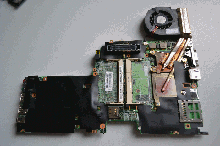
In a Thinkpad X60, the bootflash chip, also called a Firmware Hub
(FWH), is an SPI chip located on the mainboard, on an LPC bus
connected to the southbridge. It should be labelled something like
MX25L1605D, and it’s directly adjacent to some Lenovo chip called a
U72 PMH-7, the latter of which is an embedded ASIC power
management controller, the largest chip in the area and not important for our
purposes, however useful for locating the bootflash chip. Both are near the
two adjacent USB hubs:

The chipnames from the labels in the above photo can also be seen in this block diagram, and here’s a closeup of the section from that diagram pertaining to that LPC bus.
Peter responded with the following explanation of SPI versus FWH:
How to access the boot flash has changed over time; originally it was all paralell on an ISA bus, then came LPC, a 4-bit wide serial bus designed by intel, with two different and incompatible commands (yay!) for reading memory at a 32-bit address, one called “memory read”, the other called “firmware memory read”.
Intel made chipsets which required the latter and flash chips which responded to the latter, and called such flash chips a “firmware hub”. Other chipset and flash chip makers instead used the “memory read” command and didn’t invent any particular names for their flash chips. They’re generally called LPC flash, although that’s technically accurate for an FWH chip as well.
Then came SPI, the 1-bit wide serial interconnect mostly used today to save on PCB traces. To be fair, SPI was originally designed by motorola for interconnecting microcontroller peripherals. “Serial Peripheral Interconnect” the same is probably true for the memory access protocol used in PCs now.
So SPI and FWH are mutually exclusive. The X60 schematic and PCB is from a time just before SPI became the norm so it was designed to use either SPI or FWH, but in practice I’ve only seen SPI used.
U72 is the identifier in the schematic for the PMH-7 chip. (U means it’s some sort of integrated circuit and 72 means it’s the 72nd IC) I’d just refer to the lenovo chip as PMH-7.
How do I pull the chip?
The simple way is to pull the factory chip is to cut the pins, as close to the chip packaging as possible, then desolder the remaining eight pin stubs. And finally, use a desoldering wick to cleanup whatever mess is leftover.
Is there a size limit to the new chip? Can I just use a 64MB chip?
The size of the bootflash chip is limited by the SPI protocol. The largest chip which can be used is 16MB.
While it would be nice to use a huge chip, so that we have extra room for a larger kernel and initramfs, the SPI addressing scheme only has 24 bits, which limits the size of the replacement bootflash chip. It seems whichever old Unix-beardos back in the Epoch days designed the SPI protocol couldn’t foresee anyone ever wanting anything larger. (Futureproofing, assholes. It’s a thing.)
How do I flash a Linux kernel and initramfs to the new, larger chip?
Compiling a Linux kernel
“Any project whose instructions begin with
‘First, compile a kernel…’is not a project you want to be doing.”
I don’t remember who told me this, but whatever, doesn’t matter. They were totally wrong. Fuck you, Dad, I do what I want! I’m not mowing the lawn.
So… first, compile a Linux kernel. If you’ve never done this, please don’t ask me for help. While kernel hackers certainly are not known for their documentation prowess, there are plenty of tutorials on the internet to help you with this step. I remember finding these resources helpful. You also can have a look at my kernel build scripts (beware, I’ve not used that script to build a kernel image for a coreboot ROM yet); perhaps it will help.
You’ll want to strip down your kernel as small as possible (i.e. by removing drivers/support for hardware/devices which don’t exist in your machine). And, preferably, compile it monolithically (all modules compiled in, and support for additional module loading disabled). If you really want module support for some reason, it could be interesting to look into the kernel module signing features which were added into Torvald’s main tree during the 3.7 release.
Peter wrote:
The kernel file needed is called bzImage, that’s the actual filename. After running
makeit’s inarch/x86/boot/bzImagein the kernel source tree and it is the file bootloaders normally use, grub as well as lilo.
Adding an initramfs into the kernel
Additionally, while compiling the kernel, there are options to specify the
location of an
initramfs
which will get compiled into the kernel (you’ll hit these when you edit the
kernel config, e.g. when you do make-menuconfig or make-config):
 CONFIG_BLK_DEV_INITRD=y
 CONFIG_INITRAMFS_SOURCE="/usr/src/initramfs"
There is a decent Gentoo wiki page on the directory layout requirements for building a custom initramfs. Keeping in mind, of course, that your whole coreboot + kernel + initramfs will need to be small enough to flash onto the chip later.
TODO: My current, statically-linked, tor-0.2.4.20 binary is 8MB, and stripping the object symbols with
strip --strip-all '/path/to/tor-0.2.4.20'I can get it down to 1.8MB. It would be nice to see if we can get a working kernel for a Thinkpad X60, with an initramfs which includes basic security and communications software such as Tor, xmpp-client, gnupg, and, most likely, ssh, cryptsetup, and a busybox as well.
Compiling the kernel into a CoreBoot ROM
Then compile the kernel into a CoreBoot ROM. There isn’t much documentation
of this process yet, but my understanding from looking over the CoreBoot
source tree would be to use the PAYLOAD_LINUX option in
the included Kconfig file
to specify the path to the bzImage of your compiled kernel. If you try this
before I get a chance to, it would be great if you could document the steps
involved and send them to me and I’ll add them here.
Peter added:
Indeed making coreboot use a kernel as payload is done during coreboot ‘make menuconfig’ (or make config if you prefer) by entering the Payload submenu, selecting “A Linux payload” and specifying the path to the bzImage file in the kernel source tree.
How can I sign the kernel which gets flashed to the new chip?
This needs to be researched further. Likely, commands for this could be
placed directly into the initramfs’s /init script. As mentioned above, the
kernel itself supports module signing, though this is neither sufficient nor
necessary given the benefits of a monolithic kernel in this context. It could
be possible to get a TPM chip (see the tpm_tis kernel module) to keep keys
required for checking a kernel signature, though I know very little about TPM.
It’s also likely that someone else has already worked on this.
The kernel and initramfs in boot flash don’t strictly need to be signed because the flash chip is made read-only in hardware once they have been written to it. That hardware write protection is the root of trust. If someone has access to the hardware long enough to tamper with the flash chip then game over anyway.
One further step is possible: adding TPM support to coreboot, having coreboot measure itself and then using the TPM to unseal an encrypted kernel+initramfs. I’m not sure if that would actually have any advantages. However - the initramfs used with the kernel could, and should, check signatures of whatever it starts. That still needs to be designed. — Peter
Prior modifications
I’ll briefly cover the prior modifications. Peter was nice enough to drop me a tarball of all the images from the slides in his talk, which is fortunate because my camera and I are currently not exactly on speaking terms.
STEP 1:
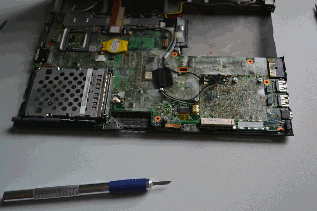
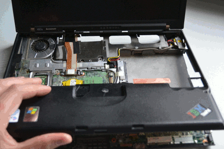
Remove the keyboard and palmrest from the chassis: 
|
|
|
STEP 2:
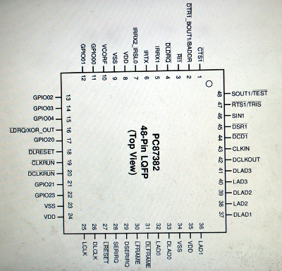
Next, disconnect pins 4, 18, 20,
26, 29, 31,
33, 37, 39, 41,
42 on a chip labelled PC87382, which forwards bus
communications through two LPC buses from an external dock. To disconnect
them, simply get a scalpel and carefully cut them from the chip’s packaging, and then desolder
the severed pins from the pads on the mainboard.
Photo 041 shows severed pins soldered into the pads. I strongly recommend to remove the pins, as I try to show in photos 043-044, to end up with a result such as in photo 045 without any pins left. This step matters because it’s significantly easier to reconnect the pins to the chip if the original pins are left on the mainboard. Someone could probably do that in an airplane lavatory, modulo the fire alarm. No pins left on the board makes it more difficult to reconnect the chip. But then again, if someone can work on the mainboard they can just replace the boot flash instead. — Peter
STEP 3:
Remove the speaker, the internal wifi card, and the 3g module (if there is one present):

STEP 4:
Remove mainboard and power adapter from chassis.

|
|
Schematic showing resistor |
STEP 5:
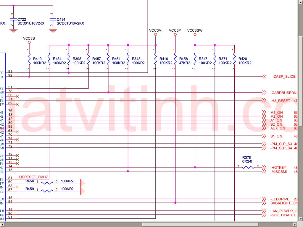
Disable the Ricoh chip in order to disable the cardbus, firewire, and sdcard reader.
To do this, lift the clear, sticky plastic protector, the one on the top of
the mainboard underneath the wifi + 3g cards, near the corner which has two
USB ports on it. Remove resistor R461, which is responsible for
controlling powerdown signal for the Ricoh
chip. Connect pin 2 of R461 (the one closest to
the USB ports) to pin 1 of R348, which is just above
R461 kind of by itself.
The lone brown component north of R461 is a capacitor, unfortunately its identifier can’t be seen in the photos because this particular PCB uses a much larger font size than most other boards I’ve seen, so the identifiers don’t fit next to their components. (There’s an AA reference north-northwest of R461 and there will be an AA legend somewhere else on that board, but that doesn’t help us much. It’s unfortunate but that’s the only board I had available when taking the photos. :) The identifiers can still be used as reference points though, as long as they aren’t mistaken for the actual identifiers for the components to be removed or modified. — Peter
When you’re done, drop the protective plastic back down over it:
STEP 6:
Remove the microphone.
The microphone is a small, round, silver thing — mostly likely underneath a sheet of opaque, black, protective plastic on the topside of the mainboard, between the firewire and USB connectors. Desolder it from the bottom of the board while pulling it out from the top with a pair of pliers.

Flashing the bootflash chip
Obtain any SPI-compatible programming interface module. Peter was using a FT4232H Mini Module with this handy looking 8-pin clamp, a Pomono 5250 8-pin test clamp to connect to the bootflash chip while it sits on the mainboard. This is the what the test clip looks like while it is attached to the bootflash chip during reflashing:

The VCC pin doesn’t need to be connected to the SPI programmer when flashing (for a Thinkpad X60) because the 3.3 volts required to power the bootflash chip is sourced from the power supply on the mainboard. When a battery or a power supply is connected to the power adapter — which should be connected to the mainboard, the bootflash chip is powered and on. Therefore, only 5 pins need to be connected to the SPI programming module.

To flash the chip, use flashrom, which is packaged in most Debian-based distros.

Flash the chip by specifying the correct chip from the ones listed during
automatic detection by flashrom, followed by the location of the binary
CoreBoot ROM:
flashrom -c MX25L1605D/MX25L1608D -r factory.bin
If you get output which reads
No EEPROM/flash device foundthen check the connection between the test clamp and the bootflash pins, and make sure you’ve specified the chip number as is written on the top of the chip.
Flashing:
flashrom -rmeans read the current contents, ie. save a backup of the factory BIOS, for future reference. Note that ThinkPad BIOSes are tied to the particular mainboard so save yours, because no other ThinkPad BIOS works on your mainboard. if you lose it and coreboot doesn’t work then you have to get another mainboard.The flashrom -w command is the one that actually writes to the chip. — Peter
How can I set write-protect on the bootflash chip from hardware?
Solder a bridge between pins 3 and 4 on the bootflash chip (MX25L1605D). My
notes say:
- pin 3 is read-protect
- pin 4 is ground
I think perhaps I meant write-protect, because read protect doesn’t make much sense to me. But that is what I wrote, in case my current second guessing turns out to be wrong.
pin 3 on the flash chip is indeed write-protect rather than read-protect.
Write-protecting the chip is a little complicated: The status register (SR) in the flash chip has a few block protect bits which say whether parts of the flash chip, or all of it, is write protected or not. The block protect bits can be changed by software as long as SR itself can be written. SR is easily written by software by sending the right command over SPI. flashrom already does this.
The top bit 0x80 in SR controls writes to SR, but software writing to SR is only completely disabled if both the 0x80 bit is set and pin 3 is connected to ground.
On Macronix and Winbond that SR 0x80 bit is non-volatile, ie. once it has been set it stays set until it is cleared by software. If pin 3 has been connected to pin 4 ground then software can’t clear the bit. On SST the SR 0x80 bit is volatile and is always 0 on reset. A workaround would be to have coreboot or possibly a program in the initramfs, but preferably coreboot, set it on boot, but this requires a bit of development.
— Peter
How can I set the write-protect bit from firmware?
The top bit in the status register (SR) is the write-protect bit, if you’re
willing to modify the flashrom program to try to set the write-protect bit
from firmware. In Peter’s output:

The output lines
  b1.SR=0x80
  b3.SR=0x82
are readings of the SR at different access times. These magic numbers mean very little to me; if it makes sense to you and you’ve got more info, let me know and I’ll add it here.
|
FINALLY…
Put it all back together and test it!
Be careful for the little wifi toggle switch on the front of the case where the lid closes down. It breaks easily. Or gets lost.
Additional Notes and Future Research
Building a kernel with an initramfs which checks the signature on a Tails live USB
If someone were to build a kernel for a CoreBoot compatible laptop which loads an initramfs, which in turn checks a signature on a Tails live USB and then calls kexec on the kernel within the Tails stick. Because the Tails .iso is signed, but not the individual components once they are installed to a USB stick, ideally, this small initramfs should support signing with keys which aren’t necessarily the Tails Signing Key (though that could be used as well, if the Tails developers would like to provide a way to obtain these additional signatures).
For coreboot machines, it would work to put the signed .iso on the USB stick and have the initramfs mount it and start kernel+initrd from within after having checked the signature of the .iso. The tails-0.20 kernel+initrd would also fit into a 16Mb boot flash. they’re about 12Mb together. I don’t know if the Tails kernel+initrd has any self-check of the root filesystem however. — Peter
Disabling the onboard ethernet controller
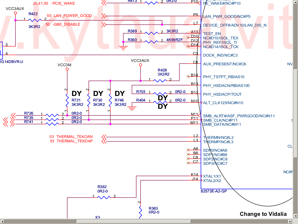
Peter mentioned in his talk that he’s been looking for a resistor on the
mainboard, labelled R422, which can be seen in the upper left of
the schematic
to the left.
It’s possible (but currently untested) that the R422 resistor could be used
to disable the onboard ethernet controller, if R422 were removed, and then
the -GBE_DISABLE side connected to ground. (Similar to R461 above.)